Thursday, November 13, 2014

60 Watt Guitar Amplifier Diagram Circuit

This design adopts a well established circuit topology for the power amplifier, using a single-rail supply of about 60V and capacitor-coupling for the speaker(s). The advantages for a guitar amplifier are the very simple circuitry, even for comparatively high power outputs, and a certain built-in degree of loudspeaker protection, due to capacitor C8, preventing the voltage supply to be conveyed into loudspeakers in case of output transistors failure. The preamp is powered by the same 60V rails as the power amplifier, allowing to implement a two-transistors gain-block capable of delivering about 20V RMS output. This provides a very high input overload capability.Amplifier circuit diagram:
60 Watt Guitar Amplifier Circuit Diagram
Amplifier parts:R1__________________6K8 1W Resistor
R2,R4_____________470R 1/4W Resistors
R3__________________2K 1/2W Trimmer Cermet
R5,R6_______________4K7 1/2W Resistors
R7________________220R 1/2W Resistor
R8__________________2K2 1/2W Resistor
R9_________________50K 1/2W Trimmer Cermet
R10________________68K 1/4W Resistor
R11,R12______________R47 4W Wirewound Resistors
C1,C2,C4,C5________47µF 63V Electrolytic Capacitors
C3________________100µF 25V Electrolytic Capacitor
C6_________________33pF 63V Ceramic Capacitor
C7_______________1000µF 50V Electrolytic Capacitor
C8_______________2200µF 63V Electrolytic Capacitor (See Notes)
D1_________________LED Any type and color
D2________Diode bridge 200V 6A
Q1,Q2____________BD139 80V 1.5A NPN Transistors
Q3_____________MJ11016 120V 30A NPN Darlington Transistor (See Notes)
Q4_____________MJ11015 120V 30A PNP Darlington Transistor (See Notes)
SW1_______________SPST Mains switch
F1__________________4A Fuse with socket
T1________________220V Primary, 48-50V Secondary 75 to 150VA Mains transformer (See Notes)
PL1_______________Male Mains plug
SPKR______________One or more speakers wired in series or in parallel Total resulting impedance: 8 or 4 Ohm Minimum power handling: 75W

Preamplifier circuit diagram:
Guitar Preamplifier Circuit Diagram
Preamplifier parts:P1,P2______________10K Linear Potentiometers
P3_________________10K Log. Potentiometer
R1,R2______________68K 1/4W Resistors
R3________________680K 1/4W Resistor
R4________________220K 1/4W Resistor
R5_________________33K 1/4W Resistor
R6,R16______________2K2 1/4W Resistors
R7__________________5K6 1/4W Resistor
R8,R21____________330R 1/4W Resistors
R9_________________47K 1/4W Resistor
R10_______________470R 1/4W Resistor
R11_________________4K7 1/4W Resistor
R12,R20____________10K 1/4W Resistors
R13_______________100R 1/4W Resistor
R14,R15____________47R 1/4W Resistors
R17,R18,R19_______100K 1/4W Resistors
C1,C4,C5,C6________10µF 63V Electrolytic Capacitors
C2_________________47µF 63V Electrolytic Capacitor
C3_________________47pF 63V Ceramic Capacitor
C7_________________15nF 63V Polyester Capacitor
C8_________________22nF 63V Polyester Capacitor
C9________________470nF 63V Polyester Capacitor
C10,C11,C12________10µF 63V Electrolytic Capacitors
C13_______________220µF 63V Electrolytic Capacitor
D1,D2____________BAT46 100V 150mA Schottky-barrier Diodes (see Notes)
Q1,Q3____________BC546 65V 100mA NPN Transistors
Q2_______________BC556 65V 100mA PNP Transistor
J1,J2___________6.3mm. Mono Jack sockets
SW1,SW2___________SPST SwitchesSensitivity:
35mV input for 40W 8 Ohm output
42mV input for 60W 4 Ohm output
Frequency response:
50Hz to 20KHz -0.5dB; -1.5dB @ 40Hz; -3.5dB @ 30Hz
Total harmonic distortion @ 1KHz and 8 Ohm load:
Below 0.1% up to 10W; 0.2% @ 30W
Total harmonic distortion @ 10KHz and 8 Ohm load:
Below 0.15% up to 10W; 0.3% @ 30W
Total harmonic distortion @ 1KHz and 4 Ohm load:
Below 0.18% up to 10W; 0.4% @ 60W
Total harmonic distortion @ 10KHz and 4 Ohm load:
Below 0.3% up to 10W; 0.6% @ 60W
Treble control:
+9/-16dB @ 1KHz; +12/-24dB @ 10KHz
Brightness control:
+6.5dB @ 500Hz; +7dB @ 1KHz; +8.5dB @ 10KHz
Bass control:
-17.5dB @ 100Hz; -26dB @ 50Hz; -28dB @ 40HzNotes:
  • The value listed for C8 is the minimum suggested value. A 3300µF capacitor or two 2200µF capacitors wired in parallel would be a better choice.
  • The Darlington transistor types listed could be too oversized for such a design. You can substitute them with MJ11014 (Q3) and MJ11013 (Q4) or TIP142 (Q3) and TIP147 (Q4).
  • T1 transformer can be also a 24 + 24V or 25 + 25V type (i.e. 48V or 50V center tapped). Obviously, the center-tap must be left unconnected.
  • D1 and D2 can be any Schottky-barrier diode types. With these devices, the harmonic modifier operation will be hard. Using for D1 and D2 two common 1N4148 silicon diodes, the harmonic modifier operation will be softer.
  • In all cases where Darlington transistors are used as the output devices it is essential that the sensing transistor (Q2) should be in as close thermal contact with the output transistors as possible. Therefore a TO126-case transistor type was chosen for easy bolting on the heatsink, very close to the output pair.
  • R9 must be trimmed in order to measure about half the voltage supply across the positive lead of C7 and ground. A better setting can be done using an oscilloscope, in order to obtain a symmetrical clipping of the output wave form at maximum output power.
  • To set quiescent current, remove temporarily the Fuse F1 and insert the probes of an Avo-meter in the two leads of the fuse holder.
  • Set the volume control to the minimum and Trimmer R3 to its minimum resistance.
  • Power-on the circuit and adjust R3 to read a current drawing of about 30 to 35mA.
  • Wait about 15 minutes, watch if the current is varying and readjust if necessary.
Author: www.redcircuits.com
ReadMore..

Heat Sensor Circuit Diagram

This simple heat sensor circuit could senses heat from various electronics device like computer, amplifier etc. and generate warning alarm. It could senses heat from environment also, but here I mention “electronics device” because it is being using mostly in electronic device to protect them from overheat.

Circuit diagram of heat sensor:

Heat
Fig-1: Schematic Circuit Diagram Of Heat/Temperature Sensor


Thermistor, 110 Ohms:

Thermistor
Fig-2: 110 Ohms Thermistor
As it is a heat sensor circuit, here a thermistor is used as a heat sensor. It is a thermal measurement device and has a variety of usages including temperature sensor/ heat sensor. The thermistor used in this circuit is a NTC (Negative Temperature Coefficient) type thermistor. When temperature increases, its resistance goes decrease. Therefore, NTC thermistor’s resistances are inverse of temperature.

Circuit Description:

You have seen, in this simple circuit diagram of heat sensor, a few number of components is used including a BC548 transistor, a 110 ohms thermistor etc.
  • BC548: BC548 is a TO-92 type NPN transistor, as its alternative you can use 2N2222, BC238, BC548, BC168, BC183 etc. they all have almost same characteristic.
  • 110 Ohms Thermistor: A 110 Ohms thermistor is used to detecting heat. I have told already about it.
  • Buzzer: A buzzer is used with +9V and collector of transistor. When the temperature/ heat exceeds a certain level then it make an alarm.
  • 4.7V Zener diode:  It is used to limit the emitter current of BC548.
  • 9V Battery: A 9V battery is used as a single power source.
  • R1, R2: A 3.3K 1/4w resistor is used as R1 and 100 ohms 1/4w as R2.
  • Switch: Here in this circuit the switch used is a simple SPST switch. You can either use the switch or not, choice is yours. It is not mandatory.
ReadMore..

Audio Test Equipment from Audio Millivoltmeter

When performing any tests on an audio system, some form of measuring device is essential. Digital multimeters are not useful, since they will not give the true picture of what is happening, and most have a fairly limited frequency range. An oscilloscope equipment is the ideal tool for audio test, but not all hobbyists can afford the outlay for a scope, and would find justifying the not inconsiderable cost a tad difficult.

An AC millivoltmeter - calibrated in dB - with a range of 30V down to 3mV full scale (80dB range) would be extremely useful. Attach a microphone (electret mic capsules are quite good), and you have a relative audio or sound level meter, even better if you have some way of calibration. The meter presented here has a very wide frequency range, and uses a switched attenuator for audio range adjustment. The attenuator uses the 30-10-3 sequence, which provides 10dB steps between ranges. The standard attenuator provides an input impedance of over 2M Ohms, but is a nuisance because with such high impedances stray capacitance causes havoc with the calibration, so a parallel capacitive attenuator is also needed. If you expect to work with valve amplifiers, you will want the high impedance, but otherwise the low impedance attenuator should do nicely.

The AttenuatorsThe two attenuator networks are shown in Figures 1 and 2, and as you can see the Hi-Z version requires all those capacitors. They must be accurate, too. Otherwise high frequency performance will be all over the place, so you need a capacitance meter or a source of close tolerance caps. The resistors are standard E24 series 1% metal film types, and the caps (if used) should ideally be polystyrene or polyester, but if ceramic is all you can get, then ceramics are what you use. If you do have to use ceramic caps, make sure that they have low thermal drift - NPO or similar.

AmplifierThe amplifier(s) used in such a audio test project are critical - we need wide bandwidth and low noise, coupled with low current drain, since we want to be able to run the meter on a 9V battery. The meter amplifier also requires high input impedance - especially for the high impedance attenuator version.

Complete Meter AmplifierThe entire audio test circuit can be built easily on a piece of perforated board (Veroboard or similar is good for this type of circuit), and a printed circuit board is quite unnecessary. Lay the physical circuit out following the schematic layout as closely as possible. This nearly always works well with discrete circuits, and makes it easy to follow 10 years later when you need to fix it. (I have had mine for nearly 20 years, and have not had to fix it yet.)

Test and CalibrationThe initial test involves connecting the meter amp to the attenuator, and applying power. All wiring must be carefully checked before you do this - the 9V batteries can supply enough current to damage the transistors, but batteries are more expensive than the transistors, and a wiring mistake may place a heavy discharge on the batteries rendering them dead before their time. Normally, batteries should last for quite a while, since the current drain is only about 4.5mA. 
ReadMore..

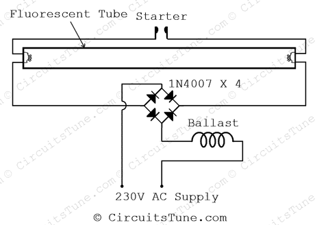
Re using fused tube light by 4 diode

A tube-light get fused due to use from a long time. You may notice that a used fluorescent tube-light get black colored on the both end of it. This circuit is to light-up those fused tube-light.
Have you think about re using a fused tube light? (Which is usually thrown out). Well here I’m showing a simple circuit using 4 diode for re-using a fused tube light.

use


The circuit diagram shown above is quite simplified from basic tube light wiring diagram by adding a bridge rectifier. Bridge rectifier provides high voltage DC to the both end of tube. All we have focused in this project is to lighting-up the weak tube using high voltage DC.

Note: A fully damaged or broken tube-light could not be light-up anyway. Use those tube-light for this project that is still trying to light-up but not fully lightened on the basic connection of tube-light.
ReadMore..

Wednesday, November 12, 2014

Long Interval Pulse Generator

A rectangular-wave pulse generator with an extremely long period can be built using only two components: a National Semiconductor LM3710 supervisor IC and a 100-nF capacitor to eliminate noise spikes. This circuit utilises the watchdog and reset timers in the LM3710. The watchdog timer is reset when an edge appears on the WDI input (pin 4). If WDI is continuously held at ground level, there are not any edges and the watchdog times out. After an interval TB, it triggers a reset pulse with a duration TA and is reloaded with its initial value. The cycle then starts all over again. As a result, pulses with a period of TA + TB are present at the RESET output (pin 10).

Circuit diagram:
long-interval-pulse-generator-circuit-diagram Long-Interval Pulse Generator Circuit Diagram

long-interval-pulse-generator-diagram

As can be seen from the table, periods ranging up to around 30 seconds can be achieved in this manner. The two intervals TA and TB are determined by internal timers in the IC, which is available in various versions with four different ranges for each timer. To obtain the desired period, you must order the appropriate version of the LM3710. The type designation is decoded in the accompanying table. 

The reset threshold voltage is irrelevant for this particular application of the LM3710. The versions shown in bold face were available at the time of printing. Current information can be found on the manufacturer’s home page (www.national.com). The numbers in brackets indicate the minimum and maximum values of intervals TA and TB for which the LM3710 is tested. The circuit operates with a supply voltage in the range of 3–5 V.
ReadMore..

Booster II for Input Impedance

The input resistance of a.c.-coupled op amp circuits depends almost entirely on the resistance with which the d.c. setting is determined. If CMOS op amps are used, the input resistance is normally high, currently up to 10 MΩ. If a higher value is needed, a bootstrap circuit may be used. This enables the input resistance to be boosted artificially to a very high value, indeed In the circuit shown in the diagram, resistor R1 sets the d.c. point for IC1a. The terminal of the resistor linked to pin 7 of IC1 would normally be at earth potential, so that the input impedance would be 10 MΩ. Connecting the other terminal of the resistor to earth via IC1a and network C2-R3-R2 as far as d.c. is concerned results in the requisite d.c. setting of the op amp.Input
Input Impedance Booster II Circuit Diagram

As far as alternating voltages are concerned, the input signal is fed back so that only a tiny alternating current flows through R1. Therefore, Rin=R1[(R2+R3)/R3]. With resistor values as specified, Rin is about 1 GΩ. One aspect must be borne in mind: the numerical value of (R2+R3)/R3 must not exceed 0.99. This means that the value of R3 cannot be less than 100 kΩ if the value of R2 is 10 MΩ. If these conditions are not met, the circuit will become unstable
ReadMore..

Saturday, November 1, 2014

Ampere or Current Booster Circuit

Volt regulators such as the LM708, and LM317 series (and others) sometimes need to provide a little bit more current then they actually can handle. If that is the case, this little circuit can help out. A power transistor such as the 2N3772 or similar can be used.
The power transistor is used to boost the extra needed current above the maximum allowable current provided via the regulator.
Current up to 1500mA(1.5amp) will flow through the regulator, anything above that makes the regulator conduct and adding the extra needed current to the output load. It is no problem stacking power transistors for even more current. (see diagram). Both regulator and power transistor must be mounted on an adequate heatsink.


Circuit diagram:


Ampere or Current Booster Circuit Diagram


Parts:

R1 = 1R-2W
R2 = 10R-2W
C1 = 35v-470uF
C2 = 35v-470uF
Q1 = TIP2955
IC1 = 78xx Regulator
ReadMore..