Showing posts with label 4. Show all posts
Showing posts with label 4. Show all posts
Thursday, November 13, 2014
Re using fused tube light by 4 diode
A tube-light get fused due to use from a long time. You may notice that a used fluorescent tube-light get black colored on the both end of it. This circuit is to light-up those fused tube-light.
Have you think about re using a fused tube light? (Which is usually thrown out). Well here I’m showing a simple circuit using 4 diode for re-using a fused tube light.
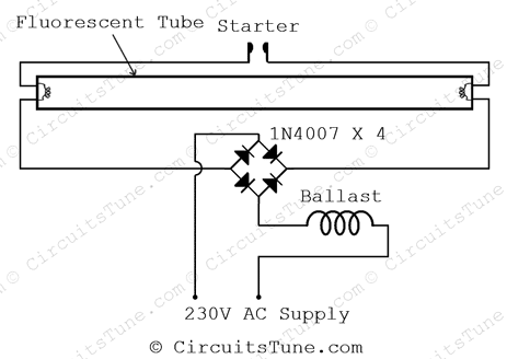
The circuit diagram shown above is quite simplified from basic tube light wiring diagram by adding a bridge rectifier. Bridge rectifier provides high voltage DC to the both end of tube. All we have focused in this project is to lighting-up the weak tube using high voltage DC.
Note: A fully damaged or broken tube-light could not be light-up anyway. Use those tube-light for this project that is still trying to light-up but not fully lightened on the basic connection of tube-light.
Have you think about re using a fused tube light? (Which is usually thrown out). Well here I’m showing a simple circuit using 4 diode for re-using a fused tube light.
The circuit diagram shown above is quite simplified from basic tube light wiring diagram by adding a bridge rectifier. Bridge rectifier provides high voltage DC to the both end of tube. All we have focused in this project is to lighting-up the weak tube using high voltage DC.
Note: A fully damaged or broken tube-light could not be light-up anyway. Use those tube-light for this project that is still trying to light-up but not fully lightened on the basic connection of tube-light.
Thursday, October 16, 2014
Simple 4 Digit Alarm Control keypad Circuit Diagram
The Simple 4 Digit Alarm Control keypad Circuit Diagram must be the kind with a common terminal and a separate connection for each key. On a 12-key pad, look for 13terminals. The matrix type with 7 terminals will NOT do. The Alarm is set by pressing a single key. Choose the key you want to use and wire it to `E`. Choose the four keys you want to use to switch the alarm off, and connect them to `A B C & D`. Your code can include the non-numeric symbols. With a 12-keypad, over 10 000 different codes are available. Wire the comm onto R1 and all the remaining keys to `F`. When `E` is pressed,current through D2 and R9 switches Q5 on.
4 digit Alarm Control keypad Circuit Diagram
![Simple]()
The relay energies, and then holds itself on by providing base current for Q5 throughR10. The 12-volt output is switched from the “off ” to the “set ”terminal, and the LED lights. To switch the Alarm off again it is necessary to press A, B, C & D in the right order. The IC is a quad 2-input AND gate, a Cmos 4081. These gates only produce a high output when both inputs are high. Pin 1is held high by R5.
This enables gate 1, so that when `A` is pressed, the output at pin 3 will go high. This output does tw1ojobs. It locks itself high using R2 and it enables gate 2 by taking pin 5 high. The remaining gates operate in the same way,each locking itself on through a resistor and enabling its successor. If the correct code is entered, pin 10 will switch Q4on and so connect the base of Q5 to ground. This causes Q5to switch off and the relay to drop out. Any keys not wired to`A B C D or E` are connected to the base of Q3 by R7. When everone of these `wrong` keys is pressed, Q3 takes pin 1 low.
This removes the `enable` from gate 1, and the code entry process fails. If `C` or `D` is pressed out of sequence, Q1 or Q2 will also take pin 1 low, with the same result. You can change the code by altering the keypad connections. If you need a more secure code use a bigger keypad with more `wrong` keys wired to`F`. A 16-key pad gives over 40 000 different codes. All components are shown lying flat on the board; but some are actually mounted upright. The links are bare copper wires on the component side. tw1o of the links must be fitted before the IC.
4 digit Alarm Control keypad Circuit Diagram

The relay energies, and then holds itself on by providing base current for Q5 throughR10. The 12-volt output is switched from the “off ” to the “set ”terminal, and the LED lights. To switch the Alarm off again it is necessary to press A, B, C & D in the right order. The IC is a quad 2-input AND gate, a Cmos 4081. These gates only produce a high output when both inputs are high. Pin 1is held high by R5.
This enables gate 1, so that when `A` is pressed, the output at pin 3 will go high. This output does tw1ojobs. It locks itself high using R2 and it enables gate 2 by taking pin 5 high. The remaining gates operate in the same way,each locking itself on through a resistor and enabling its successor. If the correct code is entered, pin 10 will switch Q4on and so connect the base of Q5 to ground. This causes Q5to switch off and the relay to drop out. Any keys not wired to`A B C D or E` are connected to the base of Q3 by R7. When everone of these `wrong` keys is pressed, Q3 takes pin 1 low.
This removes the `enable` from gate 1, and the code entry process fails. If `C` or `D` is pressed out of sequence, Q1 or Q2 will also take pin 1 low, with the same result. You can change the code by altering the keypad connections. If you need a more secure code use a bigger keypad with more `wrong` keys wired to`F`. A 16-key pad gives over 40 000 different codes. All components are shown lying flat on the board; but some are actually mounted upright. The links are bare copper wires on the component side. tw1o of the links must be fitted before the IC.
Friday, October 3, 2014
4 Ampere Regulated Power Supply 0 18V circuit
This circuit is power supply with voltage and current regulatable, with maximum current 4 Ampere for voltage range 0-18 Volt. Final power is composed by two of 2N3055.

P1 sets maximum current of power supply, if do not need or want to be able to decrease amperage, then you can remove P1 and connect P2 to the 680 Ohm resistor. P2 regulates output voltage between 0 and 18 Volt DC. P1 trims to calibrate M1 voltage meter. RFC1 and RFC2 are 50 turns 1 mm AWG on ferrite diameter 0.8 mm. The two Final transistor 2N3055 of the power supply need large heatsink for cooling.
ReadMore..
P1 sets maximum current of power supply, if do not need or want to be able to decrease amperage, then you can remove P1 and connect P2 to the 680 Ohm resistor. P2 regulates output voltage between 0 and 18 Volt DC. P1 trims to calibrate M1 voltage meter. RFC1 and RFC2 are 50 turns 1 mm AWG on ferrite diameter 0.8 mm. The two Final transistor 2N3055 of the power supply need large heatsink for cooling.
Wednesday, August 27, 2014
4 x 50 W MOSFET quad bridge power amplifier
Features
- High output power capability:
- 4 x 50 W/4 max.
- 4 x 30 W/4 @ 14.4 V, 1 kHz, 10 %
- 4 x 80 W/2 max.
- 4 x 55 W/2 @ 14.4V, 1 kHz, 10 %
- MOSFET output power stage
- Excellent 2 driving capability
- Hi-Fi class distortion
- Low output noise
- ST-BY function
- Mute function
- Automute at min. supply voltage detection
- Low external component count:
- Internally fixed gain (26 dB)
- No external compensation
- No bootstrap capacitors
- On board 0.35 A high side driver
- Output short circuit to gnd, to Vs, across the load
- Very inductive loads
- Overrating chip temperature with soft thermal limiter
- Output DC offset detection
- Load dump voltage
- Fortuitous open gnd
- Reversed battery
Circuit Diagram
 |
| 4 x 50 W MOSFET quad bridge power amplifier |
Subscribe to:
Posts (Atom)