Showing posts with label schematic. Show all posts

Friday, December 12, 2014

Lie detector schematic diagram


It's a simple lie detector that can be built in a few minutes, but can be incredibly useful when you want to know if someone is really telling you the truth. It is not as sophisticated as the ones the professionals use, but it works. It works by measuring skin resistance, which goes down when you lie.
ReadMore..

Mosfet 1000W Power Inverter schematic

circuit-schematic-power
This power inverter circuit will provide a very stable “Square Wave” Output Voltage. Frequency of operation is determined by a pot and is normally set to 60 Hz. Various “off the shelf” transformers can be used. Or Custom wind your own for best results.
ReadMore..

Amplifier Timer Schematic Diagram

amplifier-timer-schematic

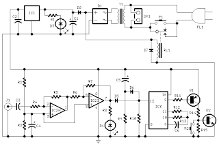
This circuit turns-off an amplifier or any other device when a low level audio signal fed to its input is absent for 15 minutes at least.Pushing P1 the device is switched-on feeding any appliance connected to SK1. Input audio signal is boosted and squared by IC2A & IC2B and monitored by LED D4.
ReadMore..

Friday, October 31, 2014

Best Performance Interruption Detector Schematic

Best Performance Interruption Detector Schematic Circuit, The circuit presented here detects interruption in security systems. Its features include no false triggering by external factors (such as sun-light and rain), easy relative positioning of the sensors and alignment of the circuit, high sensitivity, and reliability. The circuit comprises three sections, namely, transmitter, receiver, and power supply. The transmitter generates modulated IR signals and the receiver detects the change in IR intensity. Power supply provides regulated +5V to the transmitter and the receiver. 

The power supply and the speaker are kept inside the premises while the transmitter and the receiver are placed oppo site to each other at the entrance where the detection is needed. Three connections (Vcc, GND, and SPKR) are needed from the power supply/speaker to the receiver section, while only two connections (Vcc and GND) are required to the transmitter. The transmitter is basically an astable multivibrator configured around NE555 (IC3). Its frequency should match the frequency of the detector/sensor module (36 kHz for the module shown in figure) in the receiver. The transmitter frequency is adjusted by preset VR2. For making the duty cycle less than 50 per cent, di-ode 1N4148 is connected in the charging path of capacitor C7. 

The output of astable multivibrator modulates the IR signal emitted from IR LEDs that are used in series to obtain a range of 7 metres (maximum). To increase the range any further, the transmitted power has to be raised by using more number of IR LEDs. In such a case, it is advisable to use another pair of IR LEDs and 33-ohm series resistor in parallel with the existing IR LEDs and resistor R5 across points X and Y. The receiver unit consists of a monostable multivibrator built around NE555 (IC2), a melody generator, and an IR sensor module. The output of the IR sensor module goes high in the standby mode or when there is continuous presence of modulated IR signal.

Circuit diagram :

 
High-Performance Interruption Detector Circuit Diagram
 
When the IR signal path is blocked, the output of the sensor module still re-mains high. However, when the block is removed, the output of the sensor module briefly goes low to trigger monostable IC3. This is due to the fact that the sensor module is meant for pulsed operation. Thus interruption of the IR path for a brief period gives rise to pulsed operation of the sensor module. Once monostable IC2 gets triggered, its output goes high and stays in that state for the duration of its pulse width that can be controlled by preset VR1. The high output at pin 3 of the monostable makes the musical IC to function. Voltage divider comprising R2 and R3 reduces the 555 output voltage to a safer value (around 3V) for UM66 operation. The du-ration of the musical notes is set by pre-set VR1 as stated earlier. 

For proper operation of the circuit, use 7.5V to 12V power supply. A battery backup can be provided so that the circuit works in the case of power failure also. Potmeter VR3 serves as a volume control. The transmitter, receiver, and power supply units should be assembled separately. The transmitter and the receiver should have proper coverings (booster) for protection against rain. The length of the wire used for connecting the IR sensor module and IR LEDs should be minimum. 

Note. 
 
The heart of the circuit is the IR sensor module (usually used in VCRs and TVs with remote); the circuit works satisfactorily with various makes of sensors. The entire circuit can be fixed in the same cabinet if the connection wires to the sensors are smaller than 1.5 meters. The reflection property of IR signals can also be used for small distance coverage. 


Sourced By: www.streampowers.blogspot.com
ReadMore..

Sunday, September 14, 2014

0 15Watt amplifier schematic

TA7066
Amplifier circuit is also very suitable when used in fm radio receiver. Supply voltage required 8 - 25 Volt DC with a maximum output power 0.15W.See Schematic below.
Read more
ReadMore..

Saturday, September 13, 2014

Simple Bells Ring Generator Circuit Schematic

This schema generates a dual-tone bells ringing similar to most door-bell units. It can be used in many applications other than door-bell. In the Notes below several options will be given in order to suit different needs. The schema as shown in the diagram generates a "Ding-tone" when P1 is pressed and a "Dong-tone" when P1 is released. IC1D is the first-tone frequency generator and IC1F generates the second-tone.

Q2, Q5 and related components act as shape and decay controls of the two tones, trying to imitate as close as possible the bells sound. Their outputs are mixed (R7 & R13), filtered (C5) and boosted by a simple class-A audio amplifier (Q3 & Q4) in order to drive the loudspeaker. The amplifier is switched-on by Q1 when P1 is pressed, then is switched-off some seconds after P1 is released: this time-delay is fixed by C1 & R2. In this way the schema will draw a negligible current when in stand-by mode.

Simple Bells Ring Generator Circuit diagram:

 bells ring generator schematic schema diagram
Bells Ring Generator Schematic Circuit Diagram

Parts:

R1,R3,R7,R9,R13_10K 1/4W Resistors
R2_______________1M5 1/4W Resistor
R4______________27K 1/4W Resistor
R5,R11__________47K 1/4W Resistors
R6,R12_________220K 1/4W Resistors
R8_______________2M2 1/4W Resistor
R10_____________33K 1/4W Resistor
C1_______________2µ2 25V Electrolytic Capacitor
C2______________47µF 25V Electrolytic Capacitor
C3,C8___________10µF 25V Electrolytic Capacitors
C4,C7___________10nF 63V Polyester Capacitors
C5,C6__________100nF 63V Polyester Capacitors
C9_______________4µ7 25V Electrolytic Capacitor
C10______________1µF 25V Electrolytic Capacitor
D1-D5_________1N4148 75V 150mA Diodes
IC1__________MC14106 or 40106 Hex Schmitt Inverter IC
Q1_____________BC337 45V 800mA NPN Transistor
Q2,Q3,Q5_______BC238 25V 100mA NPN Transistors
Q4 ____________BC327 45V 800mA PNP Transistor
PH______________Photo resistor (any type) (see Notes)
P1______________SPST Pushbutton (see Notes)
SW1_____________SPST Switch
SPKR____________8 Ohm Loudspeaker
B1______________3V Battery (two 1.5V AA or AAA cells in series etc.)
Parts added to optional modification:
R14____________220K 1/4W Resistor
R15______________1M 1/4W Resistor

Notes:
  • To obtain a "Ding-Dong" operation when pushing on P1, no matter when it is released, you must modify the schema as shown in the frame placed at the low-right corner of the schema diagram. D4 must be removed. C10 & R15 set the time-delay separating first and second tone.
  • To obtain a one-tone-only generator, wire the schema as in the optional modification, making the following changes:
  • C9 = 100nF 63V Polyester Capacitor.
  • Omit R9 to R13 & R15; C7, C8 & C10; D2, D4, D5 & Q5.
  • Connect to negative supply pins 11 & 13 of IC1 and left open pins 10 & 12.
  • An amusing application of this schema wired as in the original schematic, is to use a photo-resistor in place of P1, then placing the unit near the flashing lamps of your Christmas tree. A soft bell sound may be heard at switch-on and switch-off of the lamp chosen.
  • To obtain higher output power you may substitute R8, Q3 & Q4 with an audio amplifier IC like the LM386 or LM380. In this case power supply must be raised to 6 - 12V but at the same time R4 & R10 should be changed to adjust bell-tone frequencies.
  • Good tone frequencies are roughly 2000 and 1650Hz respectively.
  • When in stand-by mode, current drawing of the schema is 200µA @ 3V supply: therefore SW1 can be omitted.
Source: Red Free Circuit Design
ReadMore..

Monday, September 1, 2014

Schematic Power Amplifier with IC AN7117

 *notif : this circuit is mono amplifier

Anyone who uses this amplifier circuit would be surprised. Although this circuit has a small power output just 10 watts , but also issued a sound loud enough. At least match the transistor power amplifier with 60 watts. And his sound is good with low noise. Minimum voltage is 2 volt , and maximum voltage is 12 volt .

Schematic circuit power amplifier AN7117 below :


Click image to view Enlarge
ReadMore..

Sunday, August 17, 2014

5 1 surround amplifier circuit schematic

This 5.1 surround amplifier circuit schematic use the IC AN7168 as the main component from this circuit . Minimum voltage required 12V and maximum voltage 24V , I recomended it 12 V because the voltage support on are components. But if you want to better a loud sound you can raise it. 

Maximum power output 40W with impedance 4 ohm . This 5.1 surround amplifier circuit schematic also support to make surround sound or 5.1 speaker. Use this amplifier on rear speaker , left right , and center but dont use to subwoofer speaker. See 5.1 surround amplifier circuit schematic below :

Click to view large
If you want to make a 5.1 surround sound you must make 5 the circuit of 5.1 surround amplifier circuit schematic , for left and right speaker , rear left and right speaker , and center speaker. Use the subwoofer speaker with support amlplifier subwoofer circuit .


ReadMore..

Simple Indicator for Dynamic Limiter Schematic Wiring diagram

The indicator described here is specifically designed for adjusting the dynamic limiter described elsewhere in this edition and checking whether the maximum level of the reference voltage (P1) needs to be modified. Her e we use a 4 -to -16 decoder IC (type 4514) to monitor the state of the four-bit up/down counter in the limiter schema. This IC can be powered from the ±8 V supply voltages of the limiter. The limiter board has a 6-way connector (K5) that provides access to the four counter outputs and the sup-ply voltages. Connector K1 of the indicator schema can be connected to K5 on the limiter board.
 Indicator for Dynamic Limiter Schematic

One output of the 4514 goes high for each unique 4-bit combination on its inputs, while the other outputs remain logic Low. A separate current-limiting resistor is connected in series with each LED. It was not possible to use a common cathode resistor here because most LEDs have a maximum reverse blocking voltage of only 5 V, while the supply voltage here (16 V) is a good deal higher.

The 16 LEDs ar ranged in a r ow pr ov ide a ‘fluid’ indication of the control process. You can enhance the display by using different colours for the first and last LEDs, such as red for D1 (maximum gain) and green for D16 (minimum gain), with yellow for the rest of the LEDs. While observing signals from various sources (TV set, DVD, media player, etc.), you can easily use the 16 LEDS to monitor the behaviour of the limiter and adjust the setting of potentiometer P1 in the limiter schema. It must be set such that D16 only lights up at the maximum signal level. If this is not possible and D16 remains lit a good deal of the time regardless of the position of P1, it will be necessar y to increase the value of P1. Of course, it is also poss-ible to adjust P1 so the strongest signal source extends slightly above the control range of the limiter.

This schema can easily be assembled on a small piece of prototyping board. The current consumption is around 4 mA. link
ReadMore..