Showing posts with label simple. Show all posts

Wednesday, November 19, 2014

Mini and simple power amplifier


What is the meaning of the picture above? The above picture is a miniature audio amplifier and very simple. Here I will give an audio amplifier schematic is very simple which only requires a few components only, can be seen under this scheme.


See from above scheme may occur to you, certainly cheap enough to make this amplifier and quite easy to make. The above simple audio amplifier circuit using an IC as the main amplifier and accompanied by other components. IC used is S1513, which requires a supply voltage ranging from 1.5 volts to 6 volts. And only 0.1 W output power with 4 ohm impedance. For a list components can be seen below.

Part list
C1 = 100nF
C2 = 100uF
C3 = 3n3F
C4 = 1uF
C5 = 1uF
U1 = S1513

ReadMore..

Saturday, November 15, 2014

How to Build a Common-Emitter Proximity Detector

A proximity detector is gagdet that detects when an object is nearby. There are 2 ways to build a protximity detector. One is mount the IR LED and the phototransistor so that they face each other. Then the infrared light is detected by the phototransistor. If an object comes between the IR LED and the phototransistor, the light is blocked, and the phototransistor turns off.

The other way is to build a proximity detector is to mount the IR LED and the IR photodiode next to each other facing the same direction. When an object comes near the IR LED, some infrared light will bounce off the object and be detected by the phototransistor.

How to Build a Common-Emitter Proximity Detector

Parts
Phototransistor
33KΩ Resistor
330Ω Resistor
IR LED
9-volt Battery or DC Power Supply
Red LED

Schematic Diagram
Proximity Detector Circuit

ReadMore..

Wednesday, October 29, 2014

Simple Amplifier with C945 MJE340 and TIP3055

This simple amplifier does sound good quality Power output about 10 - 14 Watts with Supply voltage about 34 - 36 Volt DC. It requires a preamp in the function of it hasnt got much advance. It requires cumbersome heat up sinks and a great transformer and a enormous power supply and alert wiring, but taking part in the bottom it is enormously regular and it sounds very good. The zener diode rubbish every wave future from the power supply, But you still barely aspire a ripple of 10mV be very successful. The swell triumph the input is enlarged, so the zener diode gets free of with the intention of, but whatever swell in attendance is wish still catch the power stage. The Buffer Stage using transistor C945 , Driver Stage Using MJE340 and Booster Stage using TIP3055 . The Transistor are using NPN transitor.

Simple Amplifier using with MJE340 TIP3055 Schematic Circuit Diagram
ReadMore..

Thursday, October 16, 2014

Simple 4 Digit Alarm Control keypad Circuit Diagram

The Simple 4 Digit Alarm Control keypad Circuit Diagram must be the kind with a common terminal and a separate connection for each key. On a 12-key pad, look for 13terminals. The matrix type with 7 terminals will NOT do. The Alarm is set by pressing a single key. Choose the key you want to use and wire it to `E`. Choose the four keys you want to use to switch the alarm off, and connect them to `A B C & D`. Your code can include the non-numeric symbols. With a 12-keypad, over 10 000 different codes are available. Wire the comm onto R1 and all the remaining keys to `F`. When `E` is pressed,current through D2 and R9 switches Q5 on.

  4 digit Alarm Control keypad Circuit Diagram

Simple


The relay energies, and then holds itself on by providing base current for Q5 throughR10. The 12-volt output is switched from the “off ” to the “set ”terminal, and the LED lights. To switch the Alarm off again it is necessary to press A, B, C & D in the right order. The IC is a quad 2-input AND gate, a Cmos 4081. These gates only produce a high output when both inputs are high. Pin 1is held high by R5.

This enables gate 1, so that when `A` is pressed, the output at pin 3 will go high. This output does tw1ojobs. It locks itself high using R2 and it enables gate 2 by taking pin 5 high. The remaining gates operate in the same way,each locking itself on through a resistor and enabling its successor. If the correct code is entered, pin 10 will switch Q4on and so connect the base of Q5 to ground. This causes Q5to switch off and the relay to drop out. Any keys not wired to`A B C D or E` are connected to the base of Q3 by R7. When everone of these `wrong` keys is pressed, Q3 takes pin 1 low.

This removes the `enable` from gate 1, and the code entry process fails. If `C` or `D` is pressed out of sequence, Q1 or Q2 will also take pin 1 low, with the same result. You can change the code by altering the keypad connections. If you need a more secure code use a bigger keypad with more `wrong` keys wired to`F`. A 16-key pad gives over 40 000 different codes. All components are shown lying flat on the board; but some are actually mounted upright. The links are bare copper wires on the component side. tw1o of the links must be fitted before the IC.
ReadMore..

Tuesday, October 14, 2014

Crystal Controlled FM Transmitter Crystal FM Transmitter The FM transmitter is relatively simple to build and with only one adjustment it is ideal

The FM transmitter is relatively simple to build and with only one adjustment it is ideal for the absolute beginner. But before I continue, let me just make one thing clear. With Wide-Band deviation, the VCO is never locked in phase, only in frequency. It uses a Varicap diode to modulate an oscillator, then lock the oscillator in a Phase Locked Loop, and compare it to a crystal oscillator
Circuit Basics
The circuit follows that of a simple textbook synthesiser comprising a Voltage Controlled Oscillator (VCO), a damped Loop Filter, a Reference Oscillator (Crystal) and a Frequency Comparator.


The only difference is that I have added a frequency divider chip to divide the VCO frequency by 64. This means that if the VCO operates at 100MHz, the output from the divider will be 1.5625MHz. If the crystal oscillator is also 1.5625MHz then the loop will be "in-lock." The control voltage from the filter to the VCO steers the frequency of the VCO so that the output of the divider is ALWAYS 1.5625MHz. Any deviation from this will result in a change of the loop voltage to move the VCO back to 100MHz.

Audio frequencies are then added to the loop voltage that control the VCO frequency. It is in this way the synthesised transmitter is modulated.

Circuit Specific
I will not delve too deeply into the ins and outs of synthesisers. I have already written several pages of information about them and the stages that are needed to make a working synthesiser.


The specific circuit is shown above. The "Prescaler" (divider) chip needs to have a supply voltage of only 5v (+/- 0.25v) so the LM317 has been included. I used the LM317T due to its larger can size (and I have got a lot of them) so it will tolerate a supply voltage of greater than 13.8vDC without burning. All has been somewhat over-engineered.

IC1 (CD4001) is the crystal oscillator with an extra gate used as nothing more than a buffer stage. This feeds the frequency comparator of a CD4046 (IC2). The comparator output is filtered with a "slack- handfull" of resistors and caps to feed the VCO; a BC547. A second BC547 has been used to isolate the VCO from the antenna. Without this device the loop would have the tendency to jump out of lock if you touched the antenna. The VCO is also coupled to the divider, IC3, which can be any one of a selection of chips. MB501, SA701, SP8704 and CA12022 are all the same device.

The filter time-constant is a couple of second or so. This makes it take about one second for the loop to stabilise. If this were not the case then the modulating frequency would be seen as a frequency error and the loop would correct the error (remove the modulation). The modulation input is via a 100K resistor and 3n3 capacitor which provides the little pre-emphasis needed for an FM broadcast transmitter. If your AF input comes from a stereo encoder then remove the 3n3 since the pre-emphasis must occur BEFORE encoding. I hope to post a stereo encoder soon, but I give no promisses.

If you are one of those who likes to dissmantle circuits, then you may notice that I have used the CD4046 Signal and Reference the wrong way around - I have used the signal input for the Reference frequency and the Reference input for the signal frequency. This is because the Reference input is designed to be fed from an external source and so it will respond to small small signals (ca: 200mV) whereas the Signal input is designed to be fed from the CD4046s own CMOS logic level oscillator. IC3 is an ECL device with only 1v output signal and is therefore NOT CMOS compatible. The result of this is that the output sense of the frequency comparator is reversed! That is why the Varicap Diode (BB105) is reference to +5v and Not to Ground.
ReadMore..

Sunday, October 5, 2014

imple Home Alarm System Home Alarm System This Home Alarm System is simple secure fast and cheap Its only few components with maximum security

 The blue led connected to the pin RA3 of micro controller is used like a memory to know if the home alarm system has been activated by an event and its reset after a reactivation. The red led connected to the power supply before the 1N5406 diode is used to check the power supply connection. Of course the other 3 micro led red near the relays are used to check the output state.

ReadMore..

Thursday, October 2, 2014

Simple 12 Volt Lamp Dimmer Circuit

This is a simple design schematic for lamp. This circuit based on 555 IC that’s used to unstable oscillator. 12 volt / 2 amp lamp dimmer that can be used to dim a standard 25 watt automobile brake or backup bulb by controlling the duty cycle of 555 IC. This is a picture of the schematic;


The operation of this circuit is when the wiper of the potentiometer is at the uppermost position, the capacitor will charge quickly through both 1K resistors and the diode, producing a short positive interval and long negative interval which dims the lamp to near darkness. When the potentiometer wiper is at the lowermost position, the capacitor will charge through both 1K resistors and the 50K potentiometer and discharge through the lower 1K resistor, producing a long positive interval and short negative interval which brightens the lamp to near full intensity. The duty cycle of the 200 Hz square wave can be varied from approximately 5% to 95%. The two circuits below illustrate connecting the lamp to either the positive or negative side of the supply.

ReadMore..

Simple IC 555 DC to DC Converter Circuit

When using a digital measuring instrument with another electronic circuit it is often necessary or desirable to completely separate the supply for the meter from that for the rest of the electronics.
The ` problem can be solved by using two separate supplies, but it can also be done using a single supply and a DC—DC converter. The type of converter described here is quite compact and can deliver a current of about 50 mA. p The circuit consists of an astable multivibrator (IC1), which switches the voltage supply for a transformer (Tr!) on and off via a transistor (T1).  The transformer secondary voltage is ha|f—wave rectified and smoothed. The output voltage is then limited by zener diode D5. I The transformer used should have a ratio between the windings of 1:1. The firing transformer used for thyristors is ideal for the iob, but a  small audio transformer (frorn a pocket radio) is also suitable. The frequency and pulse width of the circuit can be adapted to the type of transformer used by means of P1 and P2. Firing transformers give the best results at frequencies of about 100 kHz, while audio trans- formers usually work best between 0.5 and 40 kHz. The transformer must, of course, be connected witl· correct polarity. The frequency is found as follows:
F 0.7x (P1 +P2+ R1 + R2) xC1
tchargg =   X    X 
tdigchargg : 0.7 X     X C1.


ReadMore..

Wednesday, October 1, 2014

Simple Variable Voltage Current Power Supply Circuit

The cost of high grade, regulated power supplies has dropped with the advent of modern lCs......
For many applications the requirements are not that stringent and a simple, discretely constructed regulator as described here will suffice. With values as shown, the output voltage is 12V and the output current is limited to 0.5 A. For applications not requiring current limiting the circuit can supply up to 1 A. The current limiting components can then be left out. The relation between input voltage, load resistance and regulated output voltage is shown in table 1. This table cé`n therefore be used to determine whether the regulation for a particular application is sufficient. The heart ofthe regulator, high- power low-frequency transistor T1, must be fitted onto an adequate heatsink. FET T3 operates as a current source with an output maximum of 11...18 m/: this limits the base current of T1, of course, but the alternative would have been a very low value resistor this would have resulted in large current .
ReadMore..

Thursday, September 18, 2014

TDA2822M Simple low power stereo amplifier

Many people may have heard of the TDA2822 before, but for those who havent, it is a small power amplifier that will drive two channels. It is usually in an 8-pin DIL package, but older versions I have seen are 14-pin or similar (there are datasheets for both variants). For simplicity though, my circuits show schematics for the 8-pin DIL package. The datasheet is here, provided by ST. This article is based along the usage of the TDA2822M variant of the chip series as it is commonly available at my supplier at least. The TDA2822 is similar, but has slightly more pins so is less used. A Few Interesting points: I have seen the TDA2822 used in commercial offerings too, based on a circuit very similar to the schematic shown. An old ghetto Blaster used this chip (the 14-pin version) and for a small old system, its performance is better than many cheap offerings today.

I have also seen this chip in use in PC speakers, a pair I got free when I brought a computer case claimed 120W PMPO. Well I wont lie like they do, this amp is only capable of 700mW per channel from a 6V power supply into 8 ohms (should be over a watt with 12V). This amp can also function well as an amp for headphones, providing 20mW into 32 ohms from 3V. I would have used it for that purpose in my main system, but unfortunately, space was limited and all I could do was run some resistors in series with the output to cut down the volume for headphones. So what have I done with these amps then? Well recently I have rebuilt a pair of speakers I had to be amplified with this amp. The speakers are quite large 4in speakers, but the TDA2822M will provide over a watt into each from the 12V PSU I am using. With built in transformer, these speakers easily impress more then most cheap walkman and PC speakers. Update: I have changed my small stereo speakers from a two TDA7052 amps to one TDA2822M amp.

This is because my TDA7052 circuit eventually failed. I guess this is so because the outputs from the TDA7052 are bridged and the removal and insertion of the 3.5mm plug that I used to connect the other speaker to the one with the amplifier circuit in would short the circuit momentary. The new circuit will make use of the TDA2822Ms non-bridged output which is still capable of nearly as much power (enough for the reason I built the speakers). The other amp I built was brought as a project kit and uses a similar circuit, the advantage of course was I didnt need to build the board. I used this amp in a small (ish) FM radio.

Dont ask how I made a stereo FM radio circuit because the circuit was just re-used from a rather sorry. It does have LW and MW too, but these dont work properly. The speakers are just simple elliptical speakers, but quality is bad at all, although it needs a regulated PSU because that digital clock I put in makes the amp hum if it runs off the same unregulated PSU.

Construction

.


.


.


On the other hand, I would recommend, especially for beginners, that you just buy a simple DC adapter (giving about 12V). This is already made and rectified, and most importantly, safe becausemains electricity is dangerous. Get one with a good current output though, I would say 100mA is the absolute minimum, although this amp runs off a 9V PP3 longer than you would expect. For those who want a bit more volume, get a 12V PSU which will provide 1A or more (although more is probably unnecessary), and connect speakers that are sensitive to it, like those elliptical speakers in my radio, or better. Small low cost speakers (especially 55mm or less) have low sensitivity, as do high quality hi-fi speakers and should be avoided unless they are necessary.

This amp can also be very portable, as before I built the radio, I used the amp in a small pair of Walkman type speakers (that were passive). Only from 3V, there was a lot more volume then having them just passive, I recall people were quite impressed (although as you can guess the tone from the speakers was poor). Extra (simple) parts you may want to add to the schematic could be: 3.5mm jack input socket A power switch Batteries 2.1mm power plug (for external PSUs) - if wired correctly, this should disconnect the batteries when a plug is pushed into the socket. Bridge Version There is a bridge variant of this chip available in the datasheet should it be required. It is smaller still then the stereo version of the chip and should provide output levels similar to or even greater then, the TDA7052. .
Again, this circuit is simply taken from the datasheet and you may need to modify it to include a single gang volume control. Please refer to the datasheet for schematics, components their values. Thats about all that can be said about this amp because so many applications are possible from it - it is very cheap too, however if you want that extra power, using two TDA7052 amps is also simple and will give you a little more power. Remember that the TDA7052 amplifiers are bridged and may not be suitable for some situations.

Copyright Site design, content and images © Daniel Clarke 2004 Construction made using JHTMLEd - copyright © Daniel Clarke 2004
Article from::: www.electro-dan.co.uk Read More at : http://www.electro-dan.co.uk/electronics/TDA2822.html
ReadMore..

Saturday, September 13, 2014

Simple Bells Ring Generator Circuit Schematic

This schema generates a dual-tone bells ringing similar to most door-bell units. It can be used in many applications other than door-bell. In the Notes below several options will be given in order to suit different needs. The schema as shown in the diagram generates a "Ding-tone" when P1 is pressed and a "Dong-tone" when P1 is released. IC1D is the first-tone frequency generator and IC1F generates the second-tone.

Q2, Q5 and related components act as shape and decay controls of the two tones, trying to imitate as close as possible the bells sound. Their outputs are mixed (R7 & R13), filtered (C5) and boosted by a simple class-A audio amplifier (Q3 & Q4) in order to drive the loudspeaker. The amplifier is switched-on by Q1 when P1 is pressed, then is switched-off some seconds after P1 is released: this time-delay is fixed by C1 & R2. In this way the schema will draw a negligible current when in stand-by mode.

Simple Bells Ring Generator Circuit diagram:

 bells ring generator schematic schema diagram
Bells Ring Generator Schematic Circuit Diagram

Parts:

R1,R3,R7,R9,R13_10K 1/4W Resistors
R2_______________1M5 1/4W Resistor
R4______________27K 1/4W Resistor
R5,R11__________47K 1/4W Resistors
R6,R12_________220K 1/4W Resistors
R8_______________2M2 1/4W Resistor
R10_____________33K 1/4W Resistor
C1_______________2µ2 25V Electrolytic Capacitor
C2______________47µF 25V Electrolytic Capacitor
C3,C8___________10µF 25V Electrolytic Capacitors
C4,C7___________10nF 63V Polyester Capacitors
C5,C6__________100nF 63V Polyester Capacitors
C9_______________4µ7 25V Electrolytic Capacitor
C10______________1µF 25V Electrolytic Capacitor
D1-D5_________1N4148 75V 150mA Diodes
IC1__________MC14106 or 40106 Hex Schmitt Inverter IC
Q1_____________BC337 45V 800mA NPN Transistor
Q2,Q3,Q5_______BC238 25V 100mA NPN Transistors
Q4 ____________BC327 45V 800mA PNP Transistor
PH______________Photo resistor (any type) (see Notes)
P1______________SPST Pushbutton (see Notes)
SW1_____________SPST Switch
SPKR____________8 Ohm Loudspeaker
B1______________3V Battery (two 1.5V AA or AAA cells in series etc.)
Parts added to optional modification:
R14____________220K 1/4W Resistor
R15______________1M 1/4W Resistor

Notes:
  • To obtain a "Ding-Dong" operation when pushing on P1, no matter when it is released, you must modify the schema as shown in the frame placed at the low-right corner of the schema diagram. D4 must be removed. C10 & R15 set the time-delay separating first and second tone.
  • To obtain a one-tone-only generator, wire the schema as in the optional modification, making the following changes:
  • C9 = 100nF 63V Polyester Capacitor.
  • Omit R9 to R13 & R15; C7, C8 & C10; D2, D4, D5 & Q5.
  • Connect to negative supply pins 11 & 13 of IC1 and left open pins 10 & 12.
  • An amusing application of this schema wired as in the original schematic, is to use a photo-resistor in place of P1, then placing the unit near the flashing lamps of your Christmas tree. A soft bell sound may be heard at switch-on and switch-off of the lamp chosen.
  • To obtain higher output power you may substitute R8, Q3 & Q4 with an audio amplifier IC like the LM386 or LM380. In this case power supply must be raised to 6 - 12V but at the same time R4 & R10 should be changed to adjust bell-tone frequencies.
  • Good tone frequencies are roughly 2000 and 1650Hz respectively.
  • When in stand-by mode, current drawing of the schema is 200µA @ 3V supply: therefore SW1 can be omitted.
Source: Red Free Circuit Design
ReadMore..

Wednesday, September 10, 2014

Simple Thermal Fan Controller By IC 741

The controller uses one or more ordinary silicon diodes as a sensor, and uses a cheap opamp as the amplifier. I designed this schema to use 12V computer fans, as these are now very easy to get cheaply. These fans typically draw about 200mA when running, so a small power transistor will be fine as the switch. I used a BD140 (1A, 6.5W), but almost anything you have to hand will work just as well.

Thermal Fan Controller By IC 741 Circuit diagram:
Thermal
Thermal Fan Controller Circuit Diagram


Source: ESP
ReadMore..

Simple Doorbell Controlled Porchlight Wiring diagram Schematic

Build a simple Doorbell-Controlled Porchlight Circuit Diagram. This add-on schema automatically turns on your porchlight when your doorbell rings, so you can see the person ringing the doorbell at the doorstep. This also helps to guard against burglars, who usually press the doorbell switch to confirm that there is no one at home. By turning on the porchlight, the schema will trick them into believing that someone is inside the home.

You can easily connect the schema to your doorbell. The light remains on for around 20 seconds and then turns off. This duration is enough for you to find your way in the dark to open the door. However, duration can be varied by changing the RC components (R1 and C2).

Simple Doorbell-Controlled Porchlight Circuit Diagram


When you momentarily press push-to-on DPST switch (S1), the AC mains is supplied to:
1. The doorbell via S1(b) and it rings.
2. Stepdown transformer X1 via S1(a) and it delivers 12V AC at its secondary. The secondary output is rectified by diode D1 and filtered by capacitor C1 to provide the required DC. The DC voltage triggers timer 555 (IC1) and its output at pin 3 goes high for the preset time. Simultaneosly, the relay energises and AC mains flows via its N/O contacts to switch on the porchlight bulb.

Triac 1 is wired as an automatic light controller to switch on the porchlight at night and switch it off during day. The conduction angle of triac 1 depends on the bias provided to the gate of the triac through diac 1, which, in turn, is controlled by preset VR1 and the light falling on LDR1.

Sourced By: EFY Author:  T.A. Babu
ReadMore..

Monday, September 8, 2014

Simple Telephone Tapping Indicator

This simple schema can indicate a misuse or tapping of Telephone line through a loud alarm. The schema is too simple and can be easily assembled on a common PCB. Line voltage of Telephone lines is around 48 volts DC in the On hook state. When the handset is lifted, this voltage reduces to 12 volt DC. This change in voltage level is used to activate the schema.When the switch S1 is closed, schema becomes active and the telephone enters into the armed state.

The high volt DC from the telephone line passes through R1 and VR1 and bias T1 into conduction. As a result, the collector of T1 goes to ground potential to inhibit T2 from conduction. Buzzer and LED thus remain off. When the handset is lifted, the DC voltage from the telephone lines drops to 12 volts. This turns off T1 and T2 conducts. Buzzer beeps and LED lights indicating that the telephone is using.


Setting
Connect the schema to Telephone lines using a telephone plug. The free socket of the telephone or Caller ID can be used. Close S1 and adjust VR1 till buzzer stops beeping. Lift the handset. Buzzer should sound. Otherwise, just adjust VR1 till buzzer beeps.
ReadMore..

Saturday, September 6, 2014

Simple Clock pulse Generator with CD4049

If you want to generate clock with CD4049 CMOS you can do as the follow picture.The typical resister values is 100K and Capacitor is 0.01-0.1uF.The output frequency is about 1/1.1RC ___Hz

 Simple Clock pulse Generator with CD4049 Circuit Diagram


Simple
ReadMore..

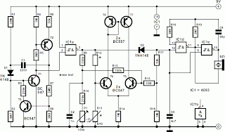
Simple Purpose Alarm

The alarm may be used for a variety of applications, such as frost monitor, room temperature monitor, and so on. In the quiescent state, the schema draws a current of only a few microamperes, so that, in theory at least, a 9 V dry battery (PP3, 6AM6, MN1604, 6LR61) should last for up to ten years. Such a tiny current is not possible when ICs are used, and the schema is therefore a discrete design. Every four seconds a measuring bridge, which actuates a Schmitt trigger, is switched on for 150 ms by a clock generator. In that period of 150 ms, the resistance of an NTC thermistor, R11, is compared with that of a fixed resistor. If the former is less than the latter, the alarm is set off.

When the schema is switched on, capacitor C1 is not charged and transistors T1–T3 are off. After switch-on, C1 is charged gradually via R1, R7, and R8, until the base voltage of T1 exceeds the threshold bias. Transistor T1 then comes on and causes T2 and T3 to conduct also. Thereupon, C1 is charged via current source T1-T2-D1, until the current from the source becomes smaller than that flowing through R3 and T3 (about 3 µA). This results in T1 switching off, so that, owing to the coupling with C1, the entire schema is disabled. Capacitor C1 is (almost) fully charged, so that the anode potential of D1 drops well below 0 V. Only when C1 is charged again can a new cycle begin.


It is obvious that the larger part of the current is used for charging C1. Gate IC1a functions as impedance inverter and feedback stage, and regularly switches on measurement bridge R9–R12-C2-P1 briefly. The bridge is terminated in a differential amplifier, which, in spite of the tiny current (and the consequent small transconductance of the transistors) provides a large amplification and, therefore, a high sensitivity. Resistors R13 and R15 provide through a kind of hysteresis a Schmitt trigger input for the differential amplifier, which results in unambiguous and fast measurement results. Capacitor C2 compensates for the capacitive effect of long cables between sensor and schema and so prevents false alarms.

If the sensor (R11) is built in the same enclosure as the remainder of the schema (as, for instance, in a room temperature monitor), C2 and R13 may be omitted. In that case,C3 willabsorb any interference signals and so prevent false alarms. To prevent any residual charge in C3 causing a false alarm when the bridge is in equilibrium, the capacitor is discharged rapidly via D2 when this happens. Gates IC1c and IC1d form an oscillator to drive the buzzer (an a.c. type). Owing to the very high impedance of the clock, an epoxy resin (not pertinax) board must be used for building the alarm. For the same reason, C1 should be a type with very low leakage current. If operation of the alarm is required when the resistance of R11 is higher than that of the fixed resistor, reverse the connections of the elements of the bridge and thus effectively the inverting and non-inverting inputs of the differential amplifier.

An NTC thermistor such as R11 has a resistance at –18 °C that is about ten times as high as that at room temperature. It is, therefore, advisable, if not a must, when precise operation is required, to consult the data sheet of the device or take a number of test readings. For the present schema, the resistance at –18 °C must be 300–400 kΩ. The value of R12 should be the same. Preset P1 provides fine adjustment of the response threshold. Note that although the prototype uses an NTC thermistor, a different kind of sensor may also be used, provided its electrical specification is known and suits the present schema.


Author: K. Syttkus
Copyright: Elektor Electronics


ReadMore..

Friday, September 5, 2014

Simple 1 5V Supply For Zn416E Circuits Wiring diagram

This regulator can be used with a +6-V source to supply ZN416E low-voltage TRF radio-receiver IC the necessary +1.5 V. R3 sets output voltage.


Simple +1.5V Supply For Zn416E Circuits Diagram

Simple

ReadMore..

A Simple MD Catridge Preamplifier

Phonographs are gradually becoming a rarity. Most of them have had to yield to more advanced systems, such as CD players and recorders or (portable) MiniDisc player/recorders. This trend is recognized by manufacturers of audio installations, which means that the traditional phono input is missing on increasingly more systems. Hi-fi enthusiasts who want make digital versions of their existing collections of phonograph records on a CD or MD, discover that it is no longer possible to connect a phonograph to the system.
Circuit diagram :
A A Simple MD Catridge Preamplifier Circuit Diagram
However, with a limited amount of schemary, it is possible to adapt the line input of a modern amplifier or recorder so that it can handle the low-level signals generated by the magnetodynamic cartridge of a phonograph. Of course, the schema has to provide the well-known RIAA correction that must be used with these cartridges. The preamplifier shown here performs the job using only one opamp, four resistors and four capacitors. For a stereo version, you will naturally need two of everything. Any stabilized power supply that can deliver ±15V can be used as a power source.
Author : H. Steeman
ReadMore..

Simple Dual Voltage Power Supply 12 Volt

This is the simple schema diagram of Dual Voltage Power Supply. It is used for Misc… application. This schema is called regulated power supply. For this reason the main component of this schema is Regulator IC. It also needs few components to built. The regulator 7812 is the positive voltage regulator and 7912 is the negative voltage regulator.

Simple Dual Voltage Power Supply 12 Volt Circuit Diagram


Simple


You can also use 7809 for 9 volt positive power supply and 7909 for negative voltage power supply. It regulates voltage from 24Volt to 12 Volt (DC). The transformer input is 110Volt to 220Volt (AC) and the output must be between 12Volt to 24Volt (AC) and current must be 500mA. In this schema some capacitors are used as a filter for removing repole.
ReadMore..

Thursday, September 4, 2014

Simple Telephone Security Device


This schema continuously checks the tel. lines and when it detects a misuse, it sounds an alarm. Additionally it transmits a loud disturbing tone through the telephone lines to prevent further misuse. The schema does not require any external power supply.


When the switch S1 is at the on position, the line voltage at the output of the rectifier diodes is approximately 48V which is enough to exceed the zeners (D5) break down voltage. So the T2 gets forward biassed. As a result the base of T1 is grounded and the remaining part of the schema doesnt get any supply. In this condition, schema draws so small current that is negligible and does not effect the normal operation of the telephone line.

When handset of any telephone connected to the line is lifted, the line voltage drops to 10V so T2 is switched off and T1 gets in forward biassed mode. The astable multivibrator schemary starts oscillating and the speaker starts sounding. The output of the astable multivibrator is also connected to the base of T1 so a loud sound is heard in the ear piece of the unauthorized telephone instrument.

ReadMore..